DNA SEQUENCER IN THE HOME: HOW TO INSTALL THE DEVICE FOR $50,000 DOLLARS
All the pictures are here
Hello everybody. My name is Alexander Sokolov, and I am an expert in quantum cryptography. I want to tell you how to make a DNA sequencer, a device for decoding deoxyribonucleic acid (DNA), at home. The market price for such a device is about $50,000 dollars.
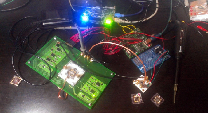 Figure 01: The “heart” of my device for reading DNA
Let me provide you a brief introduction about genetics. In 2003, a sensational declaration was made – scientists had finally decrypted the human genome. This is known as the Human Genome Project, and completion of this great international project that would allow for reading DNA was for about $3 billion dollars. The human genome is built from DNA, which is the source code (or building plan) of an organism. DNA is a double helix consisting of 4 kinds of nucleotides (Adenine, Guanine, Cytosine, and Thymine), which are repeated in the human genome about 3 billion times. As all the information on your computer is encrypted in bits, the instruction for assembling all the proteins of the human body is encrypted in the nucleotides. If we know what order the nucleotides are located in a DNA sequence, we could theoretically collect all the necessary proteins and obtain a model of a person. In fact, scientists did not decode DNA. Scientists just translated the chemical sequence into a set of zeros and ones on the computer. At the moment, we only understand the function of 5% of the genome; we can only venture to guess about the other 95%.
The cost of the first human DNA sequencing was about $100 million dollars. Over time, this figure has decreased significantly, and is now about $1000 dollars. The customer pays, the customer’s DNA is sequenced, and the laboratory gives the customer a hard drive with about 3 GB of information containing that individual’s genome in digital format.
Today, there are three main sequencers on the market. The most utilized product, HiSeq, is developed by Illumina, and provides the cheapest form of genome sequencing – fluorescent method. This method involves a laser being shined at DNA, and the newly added fluorescent-labeled nucleotides glow in response. The sequencing process requires several days, and during this time, the genomes of several people are processed. The device itself costs about $1 million dollars, and since the technology has been outdated for about 3 years (newer, cheaper, and faster sequencers have appeared), it would cost about $1000 dollars per day to pay it off.
The second device on the market by popularity literally appeared a couple of years ago. The product is called Nanopore, which is developed by Oxford Nanopore Technologies, and is based on technology that involves DNA being sequenced through a nanopore. The DNA is drawn up through the protein and electrical signals are read from it. The Nanopore is the cheapest device on the market, and is positioned as a one-time home sequencer that costs about $1000 dollars.
The third device is known as a Personal Genome Mahine (PGM), a semiconductor sequencer, that costs about $50,000 dollars. The process of sequencing the genome takes about several hours.
Figure 02: Personal Genome Mahine (PGM)
PGM was my choice and I needed it for my home laboratory, but I did not have $50,000 dollars. I therefore had to make a sequencer myself.
Before continuing, let me briefly talk about how a semiconductor sequencer works. The entire DNA chain is divided into fragments of about 300-400 nucleotides in length. These fragments are called reads, which are attached to small spheres and copied many times. Copying is necessary because this amplifies the signal from each specific read. This results in a single bundle of identical DNA fragments that "hang" onto each sphere. A set of different spheres is called a DNA library.
The heart of PGM is a disposable chip – a matrix. This matrix is similar to the matrix in a camera, but instead of having pixels reacting to light, there are pH transistors that react to changes in the pH level. The resulting DNA library is loaded onto a chip containing 10 million wells, and at the bottom of each well is a pH transistor. One sphere fits into only one hole, and consequently, only one type of read (with one specific sequence of nucleotides). The reagents are then fed to the chip in such a way that the DNA begins to copy itself in a linear manner. As a result, the nucleotides attach to the newly created chain in the order in which they stand in the original chain. Therefore, a single type of nucleotide is fed to the chip, and a change in the pH in the wells is recorded (one by one). This means that the nucleotide is attached to them. This occurs again with a different type of nucleotide being fed to the chip and changes in the pH in the wells are recorded. Thus, by feeding all 4 types of nucleotides to the chip, information can be obtained on the sequence of nucleotides in each read. Using mathematics, the short section reads are assembled on a computer into a single chain. To collect it in a confident manner, every read needs to be analyzed about 100 times.
Figure 03: Semiconductor sequencing
As we already know, the device consists of a chip, a reagent feed system, and a motherboard (detecting system). The sequencing process is carried out by the chip, whereas the rest of the device transmits certain signals to it, feeds the reagents, reads out analog signals from the chip, and digitizes and drives the resulting information stream to a computer, where data is accumulated and processed.
Figure 04: The device of the sequencer
The chip is disposable, and can be discarded after use. Such chips can be obtained for free in any quantity in places where PGM works. Why do we need them? The fact is that I already managed to use such a chip on numerous occasions. In fact, the chip is eternal. The chip can be washed, and if you remove the spheres with reads from the wells, you can use the chip again and again. If the washing is done successfully, then the quality of the work from the chip will not be different from a new chip. My idea was to make a device on the basis of this conditionally free chip.
Since there was no documentation for the integral circuit, as the manufacturer was not going to share the secrets of production, I therefore faced the task of reverse engineering the chip. To do this, I did the most obvious and simplest action – I tested the contacts with a multimeter. This would allow me to understand where the digital and analog inputs / outputs, power, and other components were located on the chip. Some information was obtained from patents on the chip, but all this of course was not enough to create a full-fledged product. I fiddled around with the chip, checked my work, and experimented with the signals. Since the chip was multi-layered, this made it difficult to trace the paths of the contact tracks, as well as allowing me to progress further on this project.
Figure 05: Chip analysis with a multimeter
Suddenly, I obtained an article from the famous blogger @BarsMonster about reverse engineering chips. I was inspired and wrote to him, as well as other enthusiasts who were engaged in photographing chips from the article. I sent them a request if it possible to take photos of the different layers of my chip. They answered that they could not do it as they could not “polish” the chip (take out the material layer by layer by a few microns). They could only photograph the top layer.
I then met an American engineer, who was also engaged in reverse engineering chips. I sent my chip to him, but the result was the same; no further information could be obtained other than photographing of the top layer.
I later came across an article on the Internet about guys whom could break the Sony PlayStation chip. I wrote to them with my questions, and immediately realized that I knew one of them. He brought his friend, who was "also engaged in genetics on an amateur level". We talked via Skype, I learned that my new friend had practical knowledge of reverse engineering chips and was ready to help. But, he did not have a necessary microscope. Therefore, I hit another road block.
A few months later, a microscope of the necessary resolution was found in a nearby laboratory, but the image quality from the built-in camera was terrible. I improvised and took photographs with a mobile phone through the microscope’s eyepiece, and was able to obtain pictures of the following quality:
Figure 06: Chip under the microscope
Finally, a suitable microscope appeared at the Quantum Center, where I worked at the moment. While I could take high quality pictures, I still had to learn how to polish the chip.
Figure 07: My working microscope
The difficulty of polishing a chip is removing layers of metal with a thickness of about 1 micron with the width of 1 centimeter. An analogous task would be avoiding an error of 10 centimeters by manually measuring the distance of1 kilometer. The results of my work are presented in the Figure 08.
Figure 08: Reverse engineering under an optical microscope
The lowest layer of silicon, the layer with transistors, and the first, second, third, and fourth layers of metal became quite visible under the microscope.
The chip consists of repeating (with the same structure) zones such as shift registers for example. This was very convenient for analyzing such pictures, and it became clear what was happening on the different layers. I reversed most of the "stuffed" areas with the abundance of logic (crossed tracks, transistors, cross-level vias), which were repeated numerous times. The most difficult part was to follow the tracks on the chip, to understand how the external contacts connected with what I have reversed, and what signals needed to be applied to which pad. Another friend of mine helped me photograph the chip layer by layer with an electronic microscope at one of the nearby Universities. The photo shoot of 1 square centimeter of the chip required about 50 GB of black and white photographs.
All the photos had to be merged into one picture. I wrote a Python program that generated an HTML file from the pictures. When I opened the file in the Opera browser, I got the results I wanted. By the way, the 10th oldest version of Opera coped with this task. I then wrote another program using JavaScript that allowed me to compare the layers, navigate between the layers, align the layers, select the scale, and perform other necessary tasks. I now had all the tools in my hands to solve the main tasks, which included tracing the tracks that pierced the chip, and restored its entire structure to the last transistor.
At the same Institute, I took another photo of the chip cut under an X-ray (see Figure 09):
Figure 09: Shooting the chip under the electronic microscope
The wells, where the spheres with the reads fall, are clearly visible. Below the wells, there are three layers of metal, and below the layers of metal is a layer with transistors.
The next task was creating of a motherboard for the chip. I designed it and sent an order for production. While waiting for the motherboard, I used a motherboard called "Marsohod-2" with FPGA. FPGA is an array of 10,000 universal logic elements. When programming with FPGA, we can get any logical scheme which easily processes gigabits of information. I wrote the firmware for FPGA as well as the dynamic management software for the system. This sets up the entire configuration for FPGA.
I then had another half-year break as I prepared an installation for the Open Innovations (Forum and Technology Show) and then went on a business trip, where I made a report on quantum cryptography at the International Conference on Luminescence and Laser Physics. Eventually, the stars aligned, and I had the motherboard ready, and the system assembled.
Figure 10: Creating the hardware
I submitted all the necessary signals to the chip and sent signals from the chip to the oscilloscope. I had the simplest oscilloscope that bought for about $100 dollars, with the firmware for about $10 dollars, which to my surprise was able to mount a picture from the signal. From the oscilloscope, I saw a picture of the chip on the screen. The picture clearly shows spots – red droplets of some reagent (see Figure 11).
Figure 11: Signal from the chip on the oscilloscope
I now had to figure out how to digitize this picture and transfer it to a computer. I therefore assembled the following installation:
Figure 12: The circuit of the device
Figure 13: The complete installation
There is a computer that provided control data to the motherboard with FPGA. The motherboard generated digital signals and sent the signals to the chip. The signals from the chip go to the amplifier and then to the analog-to-digital converter (ADC) on the motherboard. This is digitized and transmitted via the COM port to the computer. In general, the throughput of the COM port is small (about 11 kilobits per second). In one chip, there are about 1 million to 10 million "pixels", and the maximum transfer rate is 115,200 bauds. Therefore, the picture appeared on the computer in about 1.5 minutes. In the photo (Figure 14), it is clear that when a DNA library is fed to a used chip, the chip is filled non-uniformly, and less at the edges of the chip. The different colors are caused by different voltages on the pH transistors. As a result, we can clearly distinguish the holes where the spheres with ridges dropped. Later, it will help us control the flushing of the chip.
After this step was complete, the chip had to be flushed. This was necessary in order for the chip to act like a new one. Fortunately, I had another new chip as a comparative reference (Figure 14). I experimented with the fluids with different pH levels, and I obtained satisfying results.
Figure 14: Flushing the chip
In Figure 14A, we can see the new chip – the active region of the chip is almost the same color; the vertical, repeating bands are just noise. In Figure 14B, there is a used chip that has been unsuccessfully washed and it is multi-colored. Figure 14C is a used non-washed chip, and at the edges of the chip, the blue areas that are not filled with DNA completely are visible. In Figure 14D, the chip was used, but has been well-washed. This can be seen that even the gradient along the edges disappeared. Nevertheless, it would be worthwhile to prove that the chip acts like a new chip, and can be reused.
Since DNA libraries are attached to the tantalum coating of the chip in an acidic medium (with low pH), and are detached in an alkaline medium (with high pH), the chip was washed with special semi-automatic pipettes with different pH solutions (Figure 14). Based on the process, I achieved a chip cleaning precision of 83%.
You are probably asking yourself, “You completely understand the structure of the chip, but you prefer to mess around with washing used chips. Why not just produce your own chip?” The reason is that the development of the integral circuit is worth a lot of money, which can cost millions of dollars. A good chunk of this money goes to physically debugging the product, fit and adjustment of all parameters of transistors, etc. Simply copying the logic scheme is not enough. That is why I took shareware, had it already designed, manufactured, and debugged, which saved a considerable amount of money and reduced the cost of the project.
My next task was assembling an advanced device that would allow me to transfer the information to the computer faster, while at the same time, would not require a large number of separated printed circuit boards (PCBs).
Figure 15: Development of the next version of the device
I used a new motherboard with FPGA on the same chip with 2 ARM cores with Linux, a Gigabit Ethernet, and other cool features. Unlike the previous version, there was no ADC. I later designed another board with high-speed ADCs and all other necessary elements. I wrote the firmware for FPGA and the driver for Linux, which provided communication with FPGA. I then wrote a program for Linux which processed data and sent them to the PC via the Gigabit Ethernet. I tested the device, and it worked successfully.
The next task was to make a reagent feed system. I have a DNA synthesizer. In fact, it is the system for supplying reagents to the sequencer. So the idea to combine the sequencer and synthesizer into one device was born.
The next stage was to pour the chip reagents and calibrate the equipment. Reagents are unreasonably expensive, so I got a volunteer to synthesize nucleotides for my device, including protecting groups necessary for DNA synthesis and increasing the accuracy of sequencing. The main disadvantage of semiconductor sequencing is low accuracy in areas with repeated letters. For example, it is difficult to distinguish 32 from 33 A letters, since the difference in the signal is only 3%. If we join a terminate group to a nucleotide, in 1 cycle of sequencing, only one nucleotide can join at a time. If we want to join the next one, even the same nucleotide, we need to flush the chip with a special liquid to remove the blockage. This slows down the process, but improves the accuracy. Thus, the same device can use two modes - (1) sequence mode or (02) synthesize mode; in sequence mode this device can operate in (a) quick sub mode or (b) accurate sub-mode.
Another disadvantage of semiconductor sequencing is the complicated sample preparation. It is necessary to make an emulsion, in which there is only one sphere with a DNA fragment in each drop. A separate device is sold for this procedure for tens of thousands of dollars. We decided to do a sample preparation on a microfluidic chip (this is a chip with grooves through which liquids flow) and at the moment, we are experimenting with this idea.
During my work, I realize that this sequencer is slightly outdated; its heir is the S5 (developed by Thermofisher). The chip is already filmed and waiting for the reverse engineering. There is also a lot of digital stuff, and reverse engineering will take time.
An alternative direction of development is the Nanopore. I would like to assemble a team of biophysicists, which would allow it to be modernized, allowing for a reduction in the cost of sequencing.
What is this all about? The future of biotechnology, in which sequencing and editing DNA is a key to the creation of genetically modified organisms (GMOs) with specified properties, the calibration of cloning processes, and understanding the aging processes and achieving immortality in the near future.
I will be glad to talk with everyone who wants to take part in the development of this project in one way or another. You may write me to hacksequencer@gmail.com.
Thank you for your attention.
For donations: 1MRdpVoBeDfLP8hW7pXLwbxZZ2LjuagsUR (Bitcoin BTC)